Shattering the Silicon Ceiling: DR Laser Hits Milestone in Glass Substrate Packaging

Chinese equipment maker DR Laser has shipped its first panel-level Through Glass Via (TGV) laser systems, signaling a major breakthrough in glass substrate packaging for AI and semiconductor chips. The company now offers comprehensive laser solutions for both wafer-level and panel-level high-performance packaging.

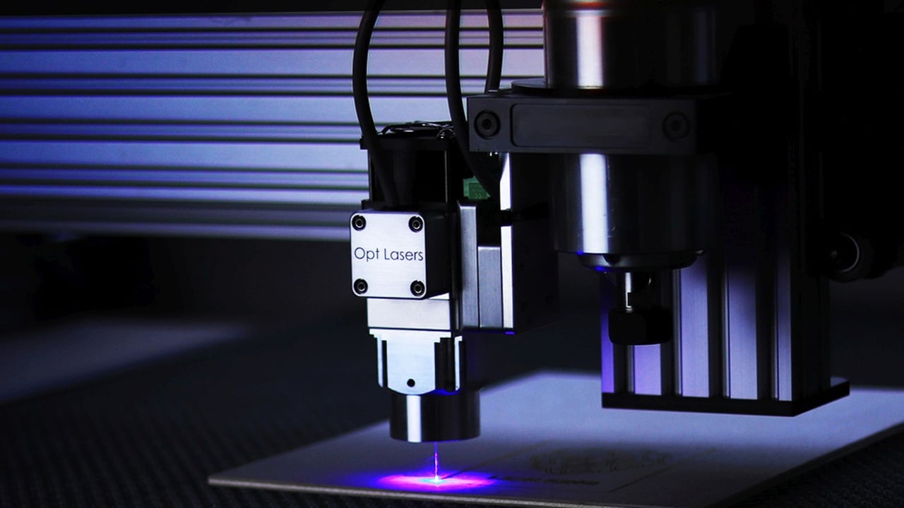
Close-up of cutting-edge laser engraving machine in a precision manufacturing process.

Key Takeaways

  • 1DR Laser has officially transitioned its TGV laser equipment from development to commercial shipment.
  • 2The technology provides full coverage across both wafer-level and panel-level packaging formats.
  • 3TGV is essential for the transition to glass substrates, which offer superior thermal and electrical properties for AI hardware.
  • 4The shipment reflects the successful diversification of DR Laser from the solar energy sector into advanced semiconductor manufacturing.

Editor's
Desk

Strategic Analysis

The significance of DR Laser’s shipment lies in the 'Glass Substrate Revolution' currently sweeping the semiconductor industry. As AI models grow more complex, traditional organic packaging is struggling with warpage and heat. Glass substrates offer the rigidity and thermal stability required for the next generation of GPU and TPU clusters. For China, developing domestic TGV equipment is a strategic imperative; it reduces reliance on Western and Japanese equipment makers in the advanced packaging segment, which has become a key battleground in the ongoing global chip war. DR Laser’s progress indicates that the technical barriers to large-format panel-level packaging are being cleared by domestic players faster than many analysts anticipated.

China Daily Brief Editorial
Strategic Insight
China Daily Brief

Wuhan DR Laser Technology (300776.SZ), a prominent player in China’s high-tech equipment sector, has announced the successful shipment of its panel-level Through Glass Via (TGV) laser micro-hole equipment. This development marks a significant step forward in the company's expansion beyond its traditional dominance in the photovoltaic sector and into the highly competitive semiconductor and advanced display packaging markets.

The TGV technology is a critical component in the next generation of chip architecture. As the semiconductor industry hits the physical limits of organic substrates, glass is emerging as the preferred material for high-performance computing and AI chips. DR Laser's equipment enables the precise drilling of microscopic holes through these glass panels, a feat necessary for creating high-density interconnections that allow for faster data transfer and better thermal management.

By achieving full coverage of both wafer-level and panel-level laser packaging technologies, DR Laser is positioning itself as a domestic alternative to international equipment giants. The shift from wafer-level to panel-level is particularly noteworthy for global manufacturers; the latter allows for significantly higher throughput and cost efficiency, as it utilizes larger rectangular areas compared to traditional circular wafers.

This move comes at a time when the global supply chain for AI hardware is under immense pressure. Tech giants like Intel and Samsung have recently accelerated their own glass substrate roadmaps to meet the demands of generative AI. DR Laser’s ability to move from the research and development phase to commercial shipment suggests that Chinese equipment manufacturers are rapidly maturing their backend semiconductor capabilities to meet domestic and potentially international demand.

Share Article

Related Articles

📰
No related articles found