As the global artificial intelligence boom pushes silicon to its physical and thermal limits, the world’s premier chipmaker, TSMC, has unveiled a new strategic framework to sustain the industry’s momentum. Speaking at the company’s 2026 Technical Symposium, Deputy Co-COO Kevin Zhang introduced a “three-layer cake” theory for AI chips, a refined hardware-centric counterpoint to Nvidia CEO Jensen Huang’s five-layer ecosystem model. While Huang’s vision spans from power grids to applications, TSMC is focusing its mastery on the physical core: compute, heterogeneous 3D integration, and the emerging frontier of optical interconnects.
TSMC is positioning silicon photonics as the most critical pillar for the next decade of AI development. Central to this strategy is the COUPE (Compact Universal Photonic Engine) technology, which utilizes 3D stacking to merge electronic and photonic integrated circuits. By bringing these components closer together, TSMC aims to eliminate the “interconnect bottleneck” that currently plagues high-performance data centers. The company reported that its first 200Gbps micro-ring modulators have already entered production, achieving a remarkably low bit-error rate that signals the readiness of light-based data transmission.
The performance implications of shifting from traditional copper wiring to optical paths are transformative. According to TSMC executives, the COUPE platform can deliver a four-fold increase in system energy efficiency and a ten-fold reduction in latency compared to conventional copper interconnects. By 2030, the company expects to reach bandwidth densities of 4TBps, representing an eight-fold leap over current capabilities. This shift is not merely an incremental upgrade but a fundamental redesign of how data moves within the massive clusters required for future Large Language Models.
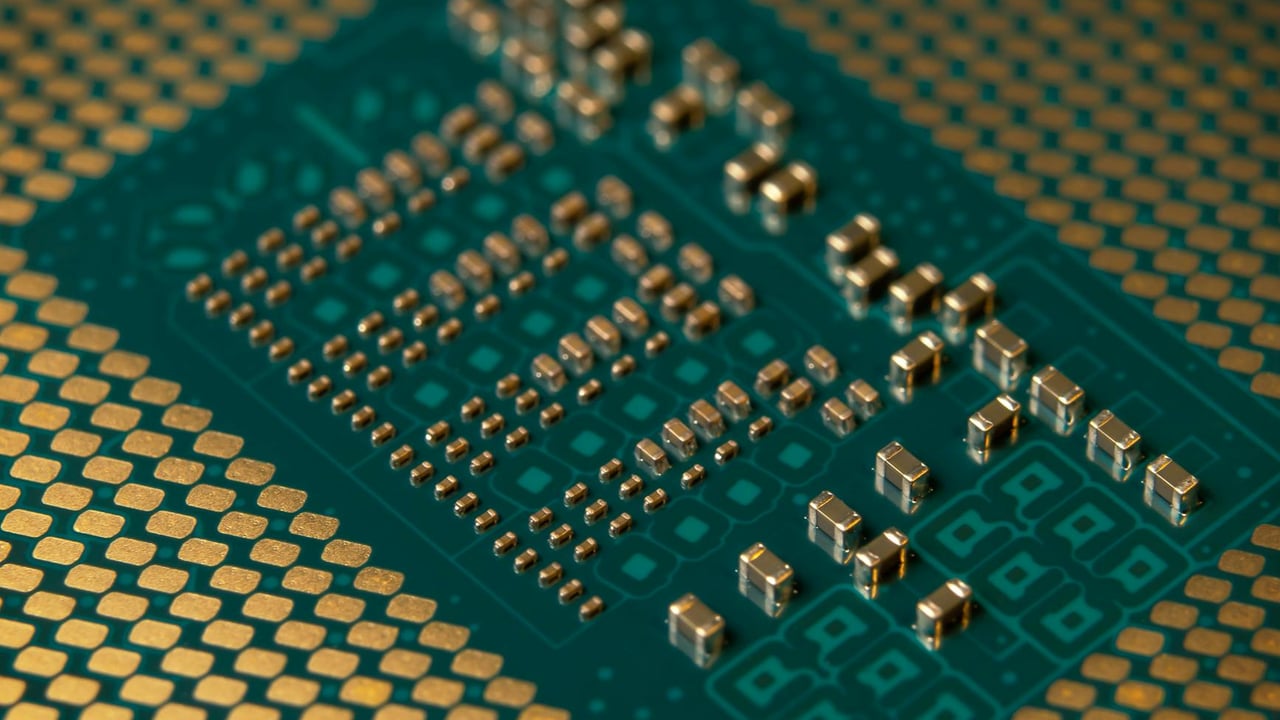
Beyond photonics, TSMC is aggressively scaling its CoWoS (Chip on Wafer on Substrate) packaging technology to accommodate the insatiable demand for memory. The roadmap revealed at the symposium indicates that by 2028, TSMC will mass-produce packaging solutions 14 times the size of a standard reticle, capable of integrating 20 High Bandwidth Memory (HBM) stacks. By 2029, this will expand further to 24 HBM stacks, effectively creating “super-chips” that function as unified, high-density computing engines. Major industry players like Nvidia and Broadcom are already reportedly queuing for these advanced capabilities.
The financial stakes are equally significant. Market analysts project that the Co-Packaged Optics (CPO) market, powered by innovations like COUPE, will reach a valuation of $10 billion by 2030. As TSMC moves from being a pure-play foundry to a holistic system integrator, its ability to master the intersection of light and electricity may decide which tech giants lead the next phase of the AI revolution. With 5.5-fold reticle size CoWoS already hitting a 98% yield, the company is demonstrating that it can execute on these complex architectures at a commercial scale.