
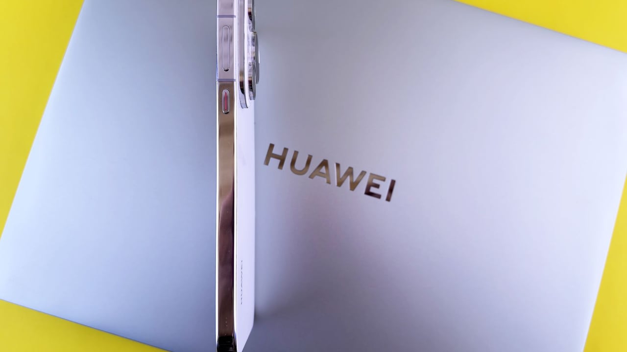

Huawei has officially introduced the 'Tao (τ) Law,' a landmark principle designed to guide the development of China’s semiconductor industry. This new framework aims to systematically reduce the time constant τ through a proprietary technique known as 'Logic Folding.' By optimizing across the device, circuit, and system levels, the strategy seeks to compress signal propagation delays and boost transistor density without the traditional reliance on extreme physical lithography processes.
Over the past six years, Huawei has quietly applied these principles to the design and mass production of 381 different chip types across various industries. The upcoming Kirin processor, scheduled for release in the fall of 2026, will be the first high-profile consumer product to implement logic folding. Initial projections suggest this architectural shift will provide a significant leap in performance, allowing Chinese hardware to remain competitive in an increasingly restricted global market.
Huawei’s long-term roadmap targets a transistor density equivalent to 1.4nm process nodes by the year 2031. This ambitious goal suggests that China is moving away from the 'follower' model of semiconductor manufacturing and toward a leadership role defined by architectural innovation. By maximizing effective computing power within limited power envelopes, the Tao Law is positioned as a critical enabler for the next wave of artificial intelligence and high-performance computing (HPC).
Investors and fund managers are already recalibrating their portfolios to align with this domestic technological pivot. Major Chinese semiconductor funds, such as those managed by Southern Fund, are heavily weighting their holdings toward domestic giants like Naura Technology and AMEC. These firms specialize in etching and advanced packaging, which are essential components of the logic folding ecosystem that Huawei is now championing as the future of Chinese silicon.