# Advanced%20Packaging
Latest news and articles about Advanced%20Packaging
Total: 17 articles found

Silicon Stronghold: How Wuxi is Rewriting China’s Semiconductor Playbook for the AI Era
Wuxi has established itself as China's third-largest semiconductor hub, leveraging its dominance in wafer fabrication and advanced packaging to capture the AI market. By investing heavily in 3D integration and domestic design capabilities, the city is positioning itself as a critical, self-sufficient node in the global chip supply chain.

The Glass Substrate Evolution: TSMC’s 2028 Roadmap and the Future of Advanced Packaging
TSMC's next-gen CoPoS packaging is expected to enter mass production in H2 2028, utilizing a hybrid structure of glass substrates and ABF film rather than a full replacement of traditional materials.

Robotic Ambitions: China Sets 2026 Deadline for Humanoid Mass Production as AI Infrastructure Shifts
China is accelerating its humanoid robotics timeline with the Tiangong 3.0, aiming for late-2026 mass production. This hardware push coincides with a global reshaping of AI infrastructure, characterized by Google diversifying its chip manufacturing to Intel and the rapid commercialization of glass substrates for advanced packaging.
The Physical Limits of Intelligence: Why AI is Transforming ‘Computing Metals’ into Strategic Assets
The global AI boom is driving a structural revaluation of 'computing metals' like copper, tin, and gallium due to massive infrastructure needs and severe supply-side constraints. Despite recent price volatility, the strategic importance of these materials is rising as resource nationalism and long mining lead times create a long-term supply-demand mismatch.
The AI Squeeze: NVIDIA’s Expansion and the Rising Costs of the Semiconductor Upstream
NVIDIA's upcoming major conference coincides with price hikes from Japanese semiconductor material suppliers, signaling a shift in market focus toward the upstream supply chain. As AI hardware demand peaks, the materials bottleneck is becoming a critical factor for the industry's sustained growth.
Reality Check for AI Speculators: Solder Giant Weiteou Dampens Advanced Packaging Hype
Shenzhen Weiteou New Materials has issued a risk warning to cool investor speculation regarding its involvement in the optical module and advanced packaging sectors. The company clarified that despite market hype, these AI-adjacent fields currently contribute very little to its total revenue.
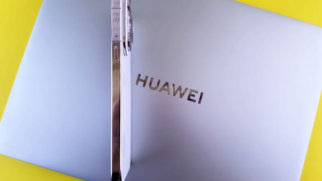
Huawei Proposes ‘Tao’s Law’ to Rewrite Semiconductor Evolution in the Post-Moore Era
Huawei has launched 'Tao’s Law' to replace Moore's Law with a focus on 'logical folding' and advanced packaging, aiming to circumvent lithography limits. Coupled with Alibaba's AI successes, these moves are driving a significant rebound in Hong Kong-listed tech stocks.
Beyond Moore’s Law: Huawei Unveils ‘Tao’ Strategy to Outrun Global Chip Sanctions
Huawei has launched the 'Tao Law,' a strategic semiconductor framework focused on 'Logic Folding' to increase chip performance and density. This architectural approach aims to achieve 1.4nm-equivalent density by 2031, providing a path for China to bypass Western restrictions on advanced lithography equipment.
Silicon’s New Foundation: The Strategic Pivot to Glass Substrates in the Global AI Race
Major semiconductor players including Apple and TSMC are shifting toward glass substrates to overcome the physical limitations of traditional chip packaging in the AI era. This transition is fueling a new investment cycle in advanced materials and precision equipment, with Chinese suppliers rapidly securing roles in the emerging global supply chain.

China’s Silicon Shield: STAR Market Chipmakers Hit Full Capacity Amid Global AI Fever
Leading Chinese semiconductor firms on the STAR Market have reported full capacity utilization for Q1, driven by surging demand for AI and automotive electronics. The industry is pivoting toward advanced packaging and specialty manufacturing to capitalize on the global AI infrastructure build-out and domestic self-sufficiency goals.
Intel’s Packaging Breakthrough Challenges TSMC’s AI Hegemony
Intel has achieved a 90% yield for its EMIB-T advanced packaging, positioning itself to win Google's next-generation TPU v8e contract. This technical milestone offers a viable alternative to TSMC's capacity-constrained CoWoS packaging for AI chip designers looking for better cost and power efficiency.
Chuangda Materials Anchors China’s Semiconductor Ambitions with New Advanced Packaging Base
Chuangda New Materials has committed 110 million RMB to build a semiconductor packaging material production line in Wuxi. The project targets the high-end materials market, aiming to produce over 2,000 tons of packaging materials annually to bolster China's domestic chip supply chain.