
# Logic%20Folding
Latest news and articles about Logic%20Folding
Total: 13 articles found

The Tao of Silicon: Huawei’s Architectural Gambit to Outrun Moore’s Law and US Sanctions
Huawei's HiSilicon has released an updated technical roadmap, the 'Tau Law' V2, detailing how 'Logic Folding' and 3D architectural innovations will allow their Kirin and Ascend chips to achieve massive performance gains despite international sanctions on advanced chipmaking equipment.

Huawei’s ‘Tao Law’ Strategy: Redefining the Semiconductor Ruler to Bypass the Lithography Wall
Huawei has introduced the 'τ (Tao) Law' as a successor to Moore's Law, pivoting the semiconductor industry from transistor shrinking to system-wide latency reduction. Through 'Logic Folding' and 3D integration, the company aims to achieve cutting-edge performance on mature manufacturing nodes, effectively bypassing Western lithography constraints.

Beyond the Nanometer: Huawei’s Radical Pivot to Transcend Moore’s Law
Huawei is shifting its semiconductor strategy away from traditional transistor miniaturization toward 'Logic Folding' and system-level efficiency. This new framework, dubbed 'Tao’s Law,' aims to achieve 1.4nm-equivalent performance by 2031 using existing manufacturing capabilities to bypass current physical and geopolitical constraints.
Huawei’s ‘Tao’ Gambit: Chasing Time to Outrun Semiconductor Sanctions
Huawei is pivoting away from traditional Moore's Law scaling in favor of the 'Tao (τ) Law,' a strategy focused on reducing signal latency through 3D stacking and architecture rather than shrinking transistors. This approach aims to achieve 1.4nm-equivalent performance by 2031 using mature lithography nodes, bypassing current Western export restrictions.
Beyond Moore’s Law: Huawei Unveils ‘Tao’ Strategy to Outrun Global Chip Sanctions
Huawei has launched the 'Tao Law,' a strategic semiconductor framework focused on 'Logic Folding' to increase chip performance and density. This architectural approach aims to achieve 1.4nm-equivalent density by 2031, providing a path for China to bypass Western restrictions on advanced lithography equipment.

Silicon Architecture as Geopolitics: Huawei’s ‘Tao’s Law’ Challenges the Moore Era
Huawei has unveiled 'Tao’s Law,' a strategic semiconductor framework that prioritizes 'Time Scaling' and 'Logic Folding' over traditional transistor miniaturization. This architectural shift aims to sustain performance gains and achieve 1.4nm-class density despite restricted access to advanced global lithography tools.

Beyond Nanometers: Huawei Unveils ‘τ Law’ in Bold Bid to Outrun Moore’s Law and US Sanctions
Huawei has introduced 'Tao’s Law' (τ Law), a semiconductor strategy that replaces traditional transistor shrinking with 'logic folding' to reduce signal latency. By focusing on time scaling rather than geometric size, Huawei aims to reach 1.4nm-equivalent performance by 2031, effectively bypassing Western lithography restrictions.
China’s Tech Titans Power A-Share Surge as Huawei Teases New Chip Breakthrough
China's tech-heavy indices saw a historic surge, with the STAR 50 rising nearly 6% and trading volume exceeding 3.2 trillion RMB. The rally was driven by Huawei's announcement of a new 'logic folding' chip technology and breakthroughs in high-performance materials for AI computing.
Beyond the Shrinking Gate: Huawei’s ‘Tau Law’ and China’s New Semiconductor Paradigm
Huawei has introduced the 'Tau Law' to challenge the dominance of Moore’s Law, focusing on architectural 'logic folding' over traditional transistor shrinkage. This move represents a strategic attempt by China to bypass Western chip sanctions and establish an independent technological trajectory.

Beyond Moore’s Law: Huawei Proposes ‘Tau Law’ as a Strategic Pivot in the Semiconductor War
Huawei has introduced the 'Tau Law' to replace Moore’s Law, focusing on time-based scaling and logic folding rather than physical miniaturization. This strategic pivot aims to achieve 1.4nm-equivalent performance by 2031, effectively bypassing current restrictions on advanced semiconductor manufacturing equipment.
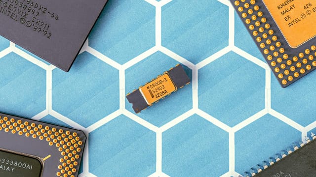
Beyond the Nanometer: Huawei’s “Tao Law” and the New Frontier of Silicon Sovereignty
Huawei has introduced the 'Tao (τ) Law,' a new semiconductor development principle that prioritizes reducing signal latency through 'logic folding' over traditional physical miniaturization. This strategy aims to achieve high-end performance parity with 1.4nm chips by 2031, effectively creating a workaround for current lithography restrictions.
Beyond Moore’s Law: Huawei Unveils ‘Tau’ Paradigm to Redefine Semiconductor Progress
Huawei has introduced 'Tau Law,' a new semiconductor design principle that prioritizes reducing signal latency and 'logic folding' over physical transistor shrinkage. The company aims to achieve performance equivalent to a 1.4nm process by 2031, effectively charting an architectural workaround to current lithography limitations.